3D DRAM may pave the way for increased density
Although pioneering semiconductor manufacturing techniques are becoming increasingly arduous to develop and the costs are soaring, the industry persistently forges ahead. As the vanguard enterprise, Taiwan Semiconductor Manufacturing Company (TSMC) has already advanced to the 3nm process node. However, not every chip witnesses a corresponding enhancement. For instance, DRAM has long grappled with scaling challenges, and researchers predict that within five years, there will be a cessation in density enhancements.
As reported by TomsHardware, Lam Research, which specializes in semiconductor circuit design, recently proffered suggestions on the evolution of DRAM products. The future ostensibly belongs to 3D DRAM, embracing a stacked architecture. It is posited that approximately another 5 to 8 years will elapse before a manufacturable 3D DRAM device emerges, bridging a three-year gap between the cessation of 2D DRAM expansion and the commencement of 3D DRAM augmentation.
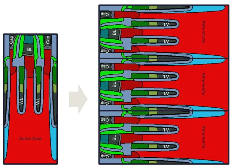
Image: Lam Research
In 3D DRAM design, paramount emphasis is placed on grappling with scaling, multilayer stacking, the miniaturization of capacitors and transistors, and interconnections between units and through-hole arrays, culminating in stipulating pertinent process requirements. The novel DRAM unit design is not a facile task of simply situating 2D DRAM components on one side and stacking them; the process constraints further exacerbate the complexity. The revamped DRAM architecture can be stacked iteratively, bearing resemblance to the NAND flash memory process, and incorporating sophisticated transistor manufacturing techniques like the GAA design.
It is understood that the inaugural 3D DRAM design can capitalize on a maximum of 28 layers of stacking. With architectural refinements and added stratification, DRAM density can achieve improvements spanning two nodes. Another encumbrance this technology faces is the current dearth of production tools that can reliably fabricate the features requisite for 3D DRAM. There’s an imperative need to enhance or even redesign DRAM production tools.
Earlier reports indicated both Samsung and SK Hynix perceive 3D DRAM as a method to surmount DRAM’s physical limitations. Samsung envisages 3D DRAM as a growth engine for the semiconductor industry, while SK Hynix believes that the electrical characteristics specifics of 3D DRAM will be disclosed next year, thus determining its developmental trajectory.


