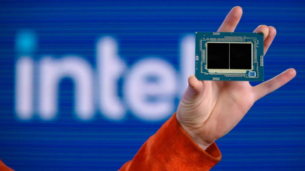
Intel is confident in the Intel 4 process
In July 2021, during the “Intel Accelerated Innovations: Process and Packaging Technology Online Conference,” Intel unveiled its latest process roadmap. The Intel 4 process node (previously known as the 7nm SuperFin) will utilize Extreme Ultraviolet (EUV) lithography, employing ultrashort wavelengths of light. This results in an approximate 20% performance enhancement per watt and advances in chip area. Furthermore, it can incorporate the next-generation Foveros and EMIB packaging technologies, offering double the transistor density compared to the Intel 7 process node.

According to The Elec, Intel representatives exuded confidence in the mass production of the Intel 4 process, believing that they can manage the intricacies of the process and have already achieved yield rates surpassing their anticipations. Contrary to the Intel 7 process node, which emphasizes performance enhancement, the Intel 4 process node prioritizes energy efficiency, proving especially beneficial for devices such as laptops.
Intel acknowledges the challenges of comparing Intel 4 with existing process nodes of other semiconductor foundries, noting that the PPA merely refers to external benchmark tests. Intel also affirmed its ample EUV lithography production capacity to meet market demands, including the upcoming Intel 3 process, with detailed plans already in place for the next few years.
Industry analysts suggest that although Intel 4 represents Intel’s inaugural foray into EUV lithography, the chips produced with the Intel 4 process surpass the performance of TSMC’s existing 5nm process and are on par with the more advanced 3nm process. Intel is poised to introduce the Meteor Lake for the consumer market, featuring a modular design and being fabricated using the Intel 4 process.


