Intel has launched a glass substrate design
In anticipation of the imminent foray into more refined manufacturing processes, Intel has unveiled a novel glass substrate design tailored for next-generation packaging technology. This design facilitates the integration of a greater number of transistors within a single package, with mass production projected between 2026 and 2030.
Intel had previously underscored the enduring relevance of Moore’s Law, emphasizing its continuous “evolution” in response to shifting computational paradigms. The newly introduced glass substrate design aims to transcend the constraints posed by organic materials. It promises superior flatness, enhanced thermal stability, and commendable mechanical rigidity, thereby augmenting the density of substrate interconnects. Such refinements fortify the stability of chip packaging, catering to dense workloads inherent to artificial intelligence, or accommodating the prodigious data throughput demands of data centers.
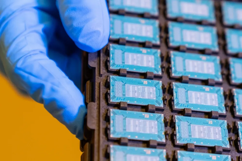
According to Intel’s elucidation, the semiconductor industry’s reliance on organic materials for packaging technology is poised to confront a transistor packaging quantity bottleneck by 2030. Concurrent challenges include power consumption, thermal expansion, and potential warping due to physical factors. Thus, the proposition of a flat, high-temperature resilient, and warp-resistant glass material for packaging substrates emerges as a superior solution.
Crafted from glass, these substrates can withstand elevated temperatures. Their intrinsic flatness enhances the focus depth of EUV lithography processes, ensuring stable coverage between densely packed layers of interconnects. This could amplify interconnect density by approximately tenfold, substantially enhancing packaging yield.
With the glass substrate design, Intel envisions the semiconductor industry, at its most expedient, to achieve the milestone of integrating one trillion transistors within a single package by 2030, realizing unparalleled packaging densities.
Transitioning from ceramic packaging in the 1990s to organic material packaging, Intel accentuates that the forthcoming era will be dominated by the potentialities unleashed by glass substrate packaging technology. Moreover, Intel takes pride in being the pioneer in achieving halogen-free and lead-free environmentally friendly packaging. They were also the industry’s trailblazers in actualizing active 3D stacked designs using cutting-edge embedded die packaging technology, underscoring their pivotal role in propelling advancements within the semiconductor realm.


