Intel will show off special E-Core chips with backside power delivery
During the “Intel Accelerates Process and Packaging Innovations” in July 2021, the company showcased a series of foundational technological innovations set to drive new product development for Intel through 2025 and beyond. Among these was the PowerVia technology, Intel’s exclusive industry-first backside power delivery network (PDN) designed to optimize signal transmission by eliminating the need for frontside power wiring. It was initially slated for introduction with the Intel 20A process node.
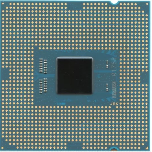
Image credit: Intel/VLSI/Twitter
As reported by Tom’s Hardware, the 2023 Symposium on VLSI Technology and Circuits will take place from June 11 to 16 in Kyoto, Japan. Intel plans to disclose its research findings on PowerVia technology during the event, presenting a specially designed chip. Employing backside power delivery, the chip features an unnamed energy-efficient core, manufactured using Intel 4 process technology, to showcase the advantages of the new technology to potential customers interested in utilizing Intel Foundry Services (IFS). As an experimental chip, it is unlikely to see mass production.
It is understood that the energy-efficient core upon which this unique chip is based may be a new architecture, speculated to be the Crestmont architecture. By utilizing PowerVia technology, the core achieves a standard cell utilization rate of over 90% in most areas, and the frequency is increased by more than 5%. Although its performance in actual workloads cannot be assessed, Intel claims the test chip achieved the expected results, displaying higher power density, which seems to indicate the effectiveness of the new technology.
Backside power delivery design helps address issues such as increased resistance in back-end-of-line (BEOL) circuits, enhancing transistor performance, and reducing power consumption. It also eliminates potential interference between data and power connections while possibly reducing area and increasing transistor density. In addition to Intel, Samsung plans to employ a technology called “BSPDN” for use in 2nm chips.


