Sony PlayStation 5 is equipped with AMD’s upgraded 6nm SoC
Since the release of the PlayStation 5, Sony has made several changes to its internal structure, mainly to reduce weight or reduce power consumption. The new version of PlayStation 5, which has recently been sold, is CFI-1202A for the optical drive version and CFI-1202B for the digital version. The corresponding weights are 3.9kg and 3.4kg, which are 300g and 200g lighter than the existing version (CFI-1102A/B), respectively, and 600g and 500g lighter than the originally released version.

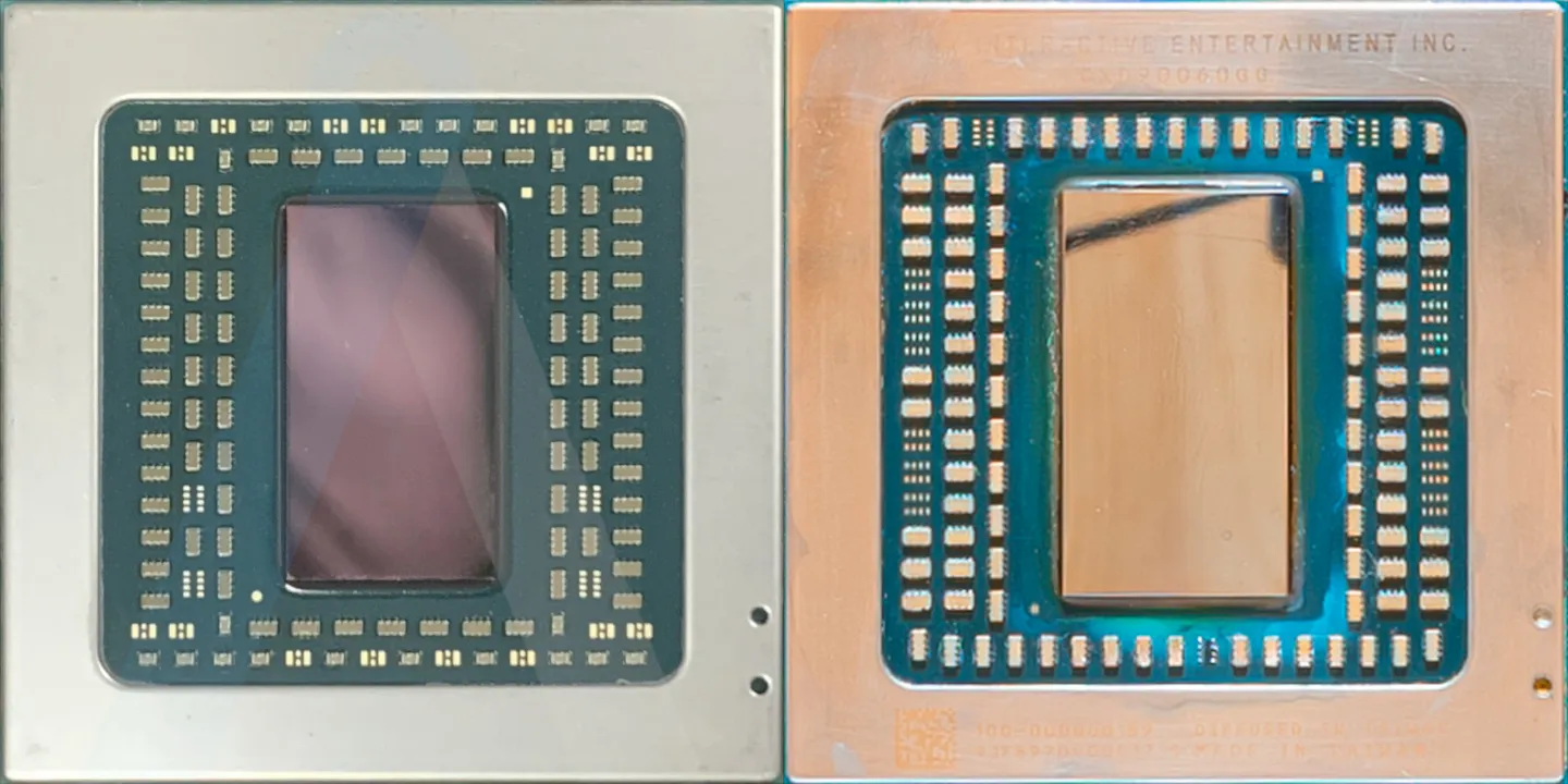
According to Angstronomics, Sony has made even bigger changes in the CFI-1202 series of PlayStation 5 consoles. Unlike the previous two, the CFI-1202 series of PlayStation 5 game consoles use a new version of AMD’s custom SoC, enabled by TSMC’s 6nm process, called “Oberon Plus”. In fact, it was reported a long time ago that Sony’s custom SoC will be changed to a 6nm process for the new PlayStation 5, but it’s faster than expected.

6nm Oberon Plus vs 7nm Oberon
Image: Angstronomics
The Size of ”Oberon Plus” has been reduced from 300 mm² to about 260 mm², a reduction of 15%, which means that each wafer can produce nearly 20% more chips at a similar cost. At the same time, the power consumption of the game console will be reduced, the corresponding cooling solution can also be simplified, and the cost can be further reduced. It is understood that in addition to changing the process, the 6nm version of the custom SoC has not made any configuration changes, and still uses the combination of Zen 2 architecture + RDNA 2 architecture.
It is estimated that the overall production cost of the new version of the PlayStation 5 game console will be reduced by about 12%, which helps Sony to recover the development costs of the project more quickly. Since the PlayStation 5 has a higher production volume than Microsoft’s Xbox Series X/S, the benefits of the conversion process will be more pronounced. The “Oberon Plus” that can be produced per wafer is nearly 50% higher than the custom chips currently used in the Xbox Series X/S, which are also expected to upgrade the process.
According to TSMC, the N6 process will increase transistor density by 18% compared to the N7 process, and can effectively reduce production and development costs with the same design rules, design infrastructure, SPICE simulation programs, and IP.


