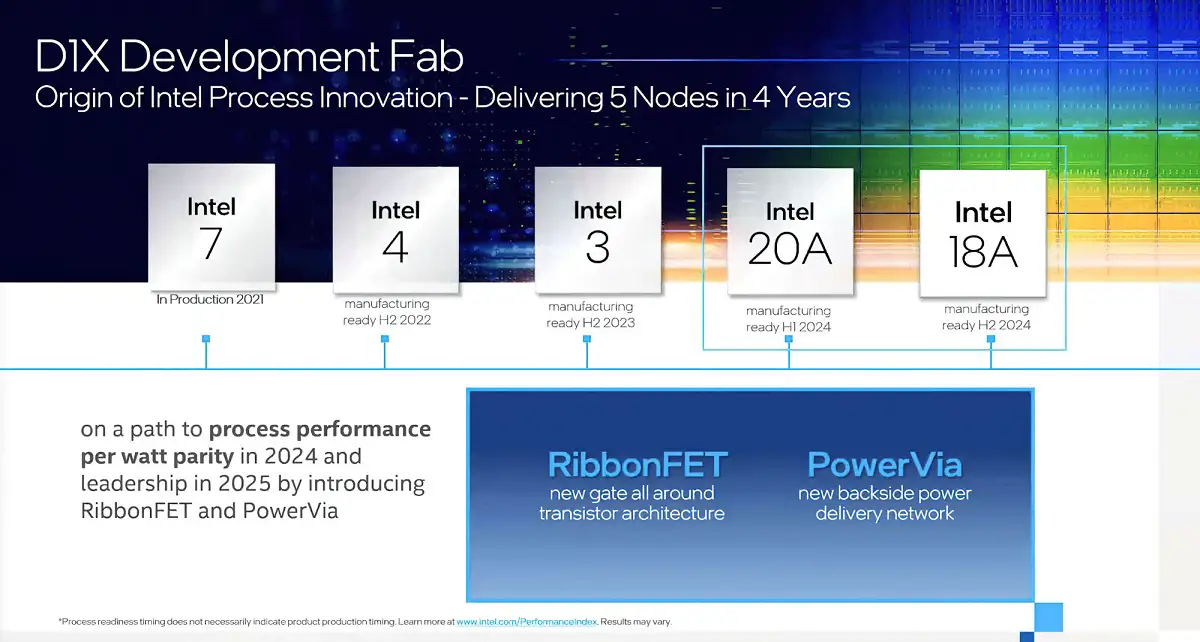
Intel may regain process technology leadership by 2025
At the “Intel Accelerated Innovation: Process and Packaging” online conference last July, Intel demonstrated a series of underlying technology innovations to drive Intel’s new product development through 2025 and beyond. In addition to announcing its first new transistor architecture RibbonFET in more than a decade and the industry’s first new backside power delivery network PowerVia, Intel also highlighted plans to rapidly adopt the next generation of extreme ultraviolet lithography (EUV) technology, high numerical aperture (High-NA) EUV, and will deploy the industry’s first High-NA EUV lithography machine.

Intel’s latest process roadmap looks very aggressive, a plan to advance five process nodes within four years. Although the performance of 12th-gen processors has improved since Pat Gelsinger returned to Intel as CEO, many people have reservations about this process roadmap given its weak performance over the past few years. Scotten Jones, president of semiconductor consulting firm IC Knowledge, recently wrote an article for SemiWiki about his journey from skepticism to confidence in Intel’s plans.


