Nvidia releases Blackwell architecture GPU: B200 and GB200
At the GTC 2024 conference held at the San Jose Convention Center in California, NVIDIA’s founder and CEO, Jensen Huang, introduced the Blackwell architecture GPU, including the B200 GPU designed to replace the H100/H200, as well as the GB200 that pairs with the Grace CPU.

The B200 is manufactured using TSMC’s improved 4NP custom process and integrates two independently manufactured dies, boasting a total of 208 billion transistors. It utilizes the new NVLink 5.0 technology to connect the two chips. The GPU comprises 160 Streaming Multiprocessors (SMs), corresponding to 20,480 cores, paired with 192GB of HBM3E memory, delivering up to 8TB/s of bandwidth and a power consumption of 700W. A single B200 GPU provides 20 petaflops of AI performance, approximately five times that of the H100’s 4 petaflops. Thanks to the second-generation Transformer engine, models can be automatically converted to the optimal format for peak performance. Moreover, the Blackwell architecture GPU supports the new FP6 format, a solution that bridges the gap between FP4 and FP8.

Details about TSMC’s 4NP process remain unspecified, but it’s unlikely to offer a significant improvement in density. The H100 was already a complete mask set, with a chip size of 814mm2, while the theoretical maximum is 858mm2. Therefore, the B200 utilizes two full mask set manufactured chips, each corresponding to four HBM3E stacks with a 1024-bit interface, 24GB capacity, and 1TB/s bandwidth. In comparison, each H100 chip corresponds to six HBM3 interfaces, meaning the B200 can allocate less chip area to memory controllers, thus dedicating more transistors to computing units. The space required for the NV-HBI interface that interconnects the two chips also occupies some area.

NVIDIA’s Superchip is designed as the quintessential platform for Artificial Intelligence (AI) and High-Performance Computing (HPC) workloads, introducing the GB200 Grace Blackwell Superchip, which combines Blackwell architecture GPUs with a Grace CPU. Equipped with two B200 GPUs and a Grace CPU, featuring 72 cores of the Arm Neoverse V2, it can be configured up to a 2700W TDP. The new platform offers 40 PetaFlops of computational performance (INT8) and boasts a vast 864GB memory pool, with HBM3E providing 16TB/s of memory bandwidth and the chips interconnected via NVLink at 3.6TB/s bandwidth.

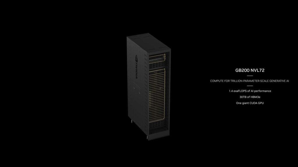
NVIDIA also unveiled the new GB200 NVL72 computing platform, a full rack solution comprising 18 1U servers. It delivers an FP8 performance of 720 petaflops and an FP4 computational power of 1440 petaflops, capable of processing up to 27 trillion AI LLM parameters. Each server contains two GB200 Grace Blackwell Superchips, totaling 36 Grace CPUs and 72 Blackwell GPUs. These compute nodes feature 1.7TB of HBM3E memory, and 32TB/s of memory bandwidth, and are all equipped with liquid-cooled MGX packaging.
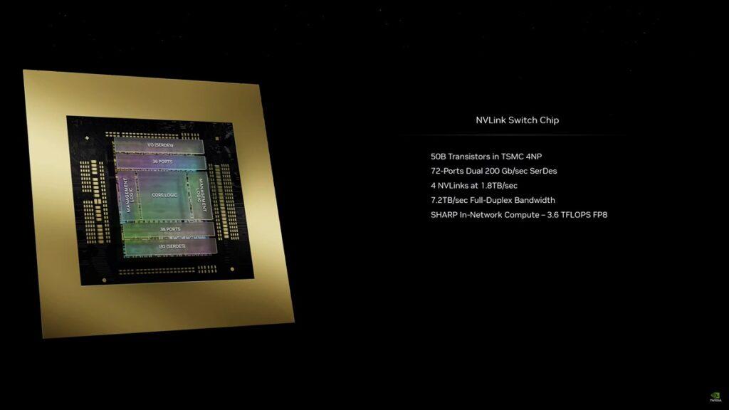
Each rack also includes a ConnectX-800G Infiniband SuperNIC and a Bluefield-3 DPU for in-network computation (80GB/s memory bandwidth). Additionally, the latest NVLINK switch, with eight interfaces and a rate of 1.8TB/s, offers a total bandwidth of 14.4TB/s. NVIDIA also launched a new NVLink Switch chip, with 50 billion transistors, manufactured using TSMC’s 4NP process, providing 7.2TB/s of bandwidth for inter-node communication.

NVIDIA has assembled a new DGX SuperPOD using eight GB200 NVL72 computing platforms, comprising a total of 288 Grace CPUs and 576 B200 GPUs. This constitutes an AI supercomputer in itself, with 240TB of memory, offering 11.5 exaflops of FP4 computational capability.

With the launch of the Blackwell architecture GPU, NVIDIA has once again solidified its leadership in the AI market, heralding a new era in AI computing. OEM manufacturers such as Dell, Cisco, HPE, Lenovo, Supermicro, Aivres, ASRock, ASUS, Eviden, Foxconn, Gigabyte, Inventec, Pegatron, Quanta, Wistron, Wiwynn, and ZT Systems will also offer their solutions in the future.


