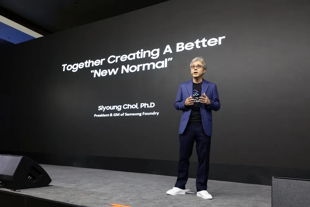
Samsung has announced that its 3nm process foundry chip products have officially shipped, and emphasized that it leads other competitors to achieve mass production of 3nm process technology. “The technology development goal down to 1.4nm and foundry platforms specialized for each application, together with stable supply through consistent investment are all part of Samsung’s strategies to secure customers’ trust and support their success,” said Dr. Si-young Choi, president and head of Foundry Business at Samsung Electronics. “Realizing every customer’s innovations with our partners has been at the core of our foundry service.”
At present, Samsung also plans to actively strive for the foundry market in the United States. In addition to the factory in Austin, Texas, it also plans to build a new factory in the nearby city of Taylor, which is expected to start operation in 2024 and plans to provide foundry mass production resources with the latest 3nm process technology.
Support Our Threat Intelligence
If you find our CVE report and cybersecurity news helpful, consider supporting our work.