Intel announced the process roadmap from now to 2025
At the just-concluded “Intel Accelerates Process and Packaging Innovations Online Conference”, Intel CEO Pat Gelsinger delivered a speech, showing a series of underlying technology innovations that will drive Intel’s new product development by 2025 and beyond. At the same time, Intel announced that AWS will be the first customer to use Intel Foundry Services (IFS) packaging solutions.
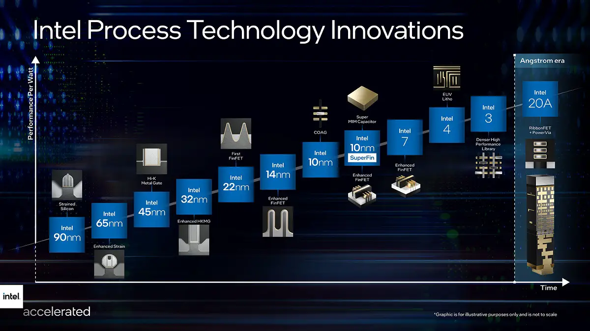
Image: Intel
At this online conference, in addition to announcing its first brand-new transistor architecture RibbonFET in more than a decade and the industry’s first brand-new backside power transmission network PowerVia, Intel also highlighted the rapid adoption of next-generation extreme ultraviolet lithography (EUV) technology plan, namely high numerical aperture (High-NA) EUV, Intel is also expected to take the lead in obtaining the industry’s first High-NA EUV lithography machine. Intel is currently accelerating its roadmap for process innovation to ensure that its process performance will once again lead the industry by 2025.
Intel said that since 1997, the traditional nano-based process node naming method no longer corresponds to the actual gate length of the transistor. With the launch of Intel Foundry Services (IFS) in the IDM 2.0 strategy, Intel decided to introduce a new naming system for its process nodes and create a clear and consistent framework to help customers have a clearer and accurate understanding of the process nodes of the entire industry.
Intel technologists described the following roadmap with the new node names and the innovations enabling each node:
- Intel 7 delivers an approximately 10% to 15% performance-per-watt increase versus Intel 10nm SuperFin, based on FinFET transistor optimizations. Intel 7 will be featured in products such as Alder Lake for client in 2021 and Sapphire Rapids for the data center, which is expected to be in production in the first quarter of 2022.
- Intel 4 fully embraces EUV lithography to print incredibly small features using ultra-short wavelength light. With an approximately 20% performance-per-watt increase, along with area improvements, Intel 4 will be ready for production in the second half of 2022 for products shipping in 2023, including Meteor Lake for client and Granite Rapids for the data center.
- Intel 3 leverages further FinFET optimizations and increased EUV to deliver an approximately 18% performance-per-watt increase over Intel 4, along with additional area improvements. Intel 3 will be ready to begin manufacturing products in the second half of 2023.
- Intel 20A ushers in the angstrom era with two breakthrough technologies, RibbonFET and PowerVia. RibbonFET, Intel’s implementation of a gate-all-around transistor, will be the company’s first new transistor architecture since it pioneered FinFET in 2011. The technology delivers faster transistor switching speeds while achieving the same drive current as multiple fins in a smaller footprint. PowerVia is Intel’s unique industry-first implementation of backside power delivery, optimizing signal transmission by eliminating the need for power routing on the front side of the wafer. Intel 20A is expected to ramp in 2024. The company is also excited about the opportunity to partner with Qualcomm using its Intel 20A process technology.
- 2025 and Beyond: Beyond Intel 20A, Intel 18A is already in development for early 2025 with refinements to RibbonFET that will deliver another major jump in transistor performance. Intel is also working to define, build and deploy next-generation High NA EUV, and expects to receive the first production tool in the industry. Intel is partnering closely with ASML to assure the success of this industry breakthrough beyond the current generation of EUV.


